
The Lab for Education & Application Prototype (LEAP) grant program is a broad coalition of AIM Photonics, government, academia, and industry that evolved as a solution to a national shortage of photonics and electronics technicians and engineers. The other challenge that LEAP solves is that small-to-medium enterprises (SMEs) do not have the tools to develop disruptive photonics products.
The LEAPS are funded by the Commonwealth of Massachusetts' M2I2 program to support AIM Photonics. They will enable (1) the fabrication of prototypes and initial proof of manufacturing and (2) the creation of new high-tech integrated photonics manufacturing jobs.
LEAP Network
$1M LEAP at MIT
The LEAP at MIT.nano is part of the AIM Photonics Academy which houses its administrative offices at MIT. “The LEAP is becoming a hub on campus for the packaging and testing of both electronic and photonic chips,” said Anuradha Agarwal, the leader of the LEAP and a principal research scientist at the MIT Materials Research Laboratory. The LEAP facility opened after being awarded additional M2I2 grants.
$4M WPI/QCC LEAP
The lab is accessible to employers from across the Commonwealth, with an emphasis on regional employers in the photonics manufacturing sector, and will engage manufacturers interested in specific product development projects or prototyping needs. The LEAP will also play a strong role in workforce training, developing curriculum with key partners that will target students at two and four year colleges, as well as at the K-12 level. WPI and QCC will collaborate with companies in the Central Mass region to inform the development of the LEAP and work with the MA Manufacturing Extension Partnership to provide access to manufacturers across Massachusetts. https://www.wpi.edu/research/core-research-facilities/leap
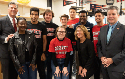
$3.8M Bridgewater State/Stonehill College LEAP
Southeastern Massachusetts Lab for Education and Application Prototypes (SEMA LEAP)
This award created a regional integrated photonics hub centered at both Stonehill College and Bridgewater State University (BSU). The project combines the complementary strengths, resources, and know-how of each institution to further technology, innovation, workforce training, and manufacturing in Massachusetts in Photonic Integrated Circuits (PICs). SEMA LEAP will train and educate photonics industry technician-level and engineering workforce to support new economic growth and development in areas such as telecommunication and data-communication, precision measurements, biomedical sensing and imaging, optic and laser development, and auto-driving.
$2.5 Million for New Advanced Manufacturing Center
Integrated Photonics Training Facility
This M2I2 grant will fund the future installation of a high-power semiconductor laser lab which will support the development of innovative technologies, and a state-of-the-art education and training facility for students, teachers, and faculty from WNE, Springfield Technical Community College (STCC), and other Massachusetts institutions seeking training in optics and photonics technology. This LEAP lab or advanced manufacturing center will be located at Convergent Photonics in Chicopee, MA.